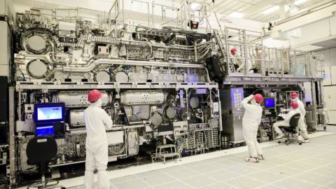
Chipmaking is tough. Like really tough. Just how tough? An engineer could spend many hours talking about the intricacies of just a single step in the lithographic or packaging process and you'd come away wiser but moderately terrified about the scale of the accomplishments required to create any and all computer chips. But a photograph speaks a thousand words, and these photos of Intel's new lithographic 'High NA EUV' machines make it quite clear how incredibly complex this whole chipmaking biz is.

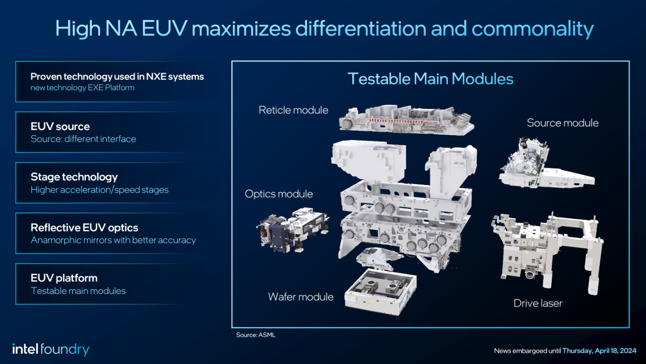
What you're looking at here is a lithography tool (just one, incredibly) called a TWINSCAN EXE:5000 High NA EUV. This $370 million machine offers Intel the new ability to scale down processors into more efficient, effective designs. 'High NA' stands for High Numerical Aperture. 'EUV' stands for Extreme Ultraviolet.
The wider chipmaking industry has been adopting EUV to allow for more continued advancement of chipmaking. Previous DUV lithographic processes only go so far, and the smaller chips are required to go, the more DUV processes are required to introduce extra steps into the manufacturing process, such as multi patterning. This adds time, complexity, and cost. That's where EUV comes in, which reduces the number of processes required again while allowing for sub-10nm process nodes. In theory, this also reduces cost, though in practice hasn't worked out that way. EUV requires extremely large and complicated tools, as you might be able to tell from the photographs below.
The important thing is it remains possible to make more complicated and better performing processors thanks to EUV. Intel uses EUV within its Intel 4 process node. TSMC has used EUV since N7+.
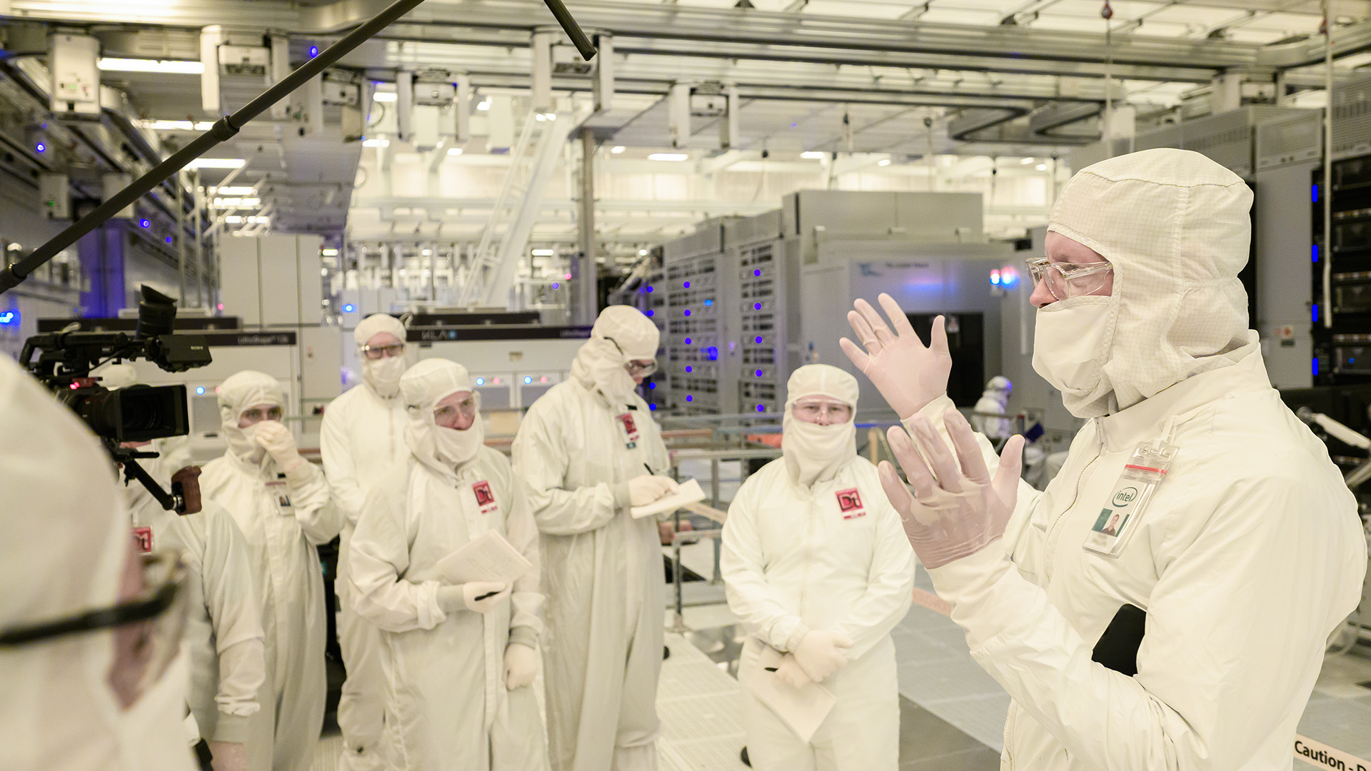
High NA EUV is a little different again. Using newer machines from ASML, the company that makes most lithographic machines out of the Netherlands, Intel is able to produce wafers quicker and enjoy higher yields per wafer (a higher proportion of processor on each wafer are usable). Mark Phillips, an Intel Fellow and Director of Lithography Hardware and Solutions, Logic Technology Development, says the increased resolution of High NA EUV allows for Intel to reduce excess steps usually required for cutting-edge chips, such as multi-patterning and the number of masks.
Altogether, High NA is just a simpler process, though you wouldn't get that impression from the scale and complexity of the machines required to do it.

High NA EUV doesn't come cheap. Intel will have to bear the brunt of using these High NA and using it effectively to get return on investment.
“The introduction of high NA will be on those few bottleneck layers, and it will continue in parallel with layers that stay on .33 NA, layers that say on 193[nm] immersion. Whatever is the cost effective technology for delivering the needs of that process layer.”

Intel is the first to get a High NA EUV machine, and it will be used on its Intel 14A and later Intel 14A-E process nodes, which the company will get to work developing from 2025. So, a good while yet until we see an Intel Core processor built using High NA EUV.
Intel is on a mission to get back into the driving seat when it comes to world-class chipmaking. To do that, it needs to leapfrog TSMC, the Taiwanese chip manufacturer currently leading the way. Intel's plan to achieve that involves “Five nodes in four years”, culminating in Intel taking back the crown from TSMC for process leadership with Intel 18A in 2025. TSMC also hopes to adopt High NA EUV, though is slower to adopt the technology, choosing instead to focus on further patterning using existing EUV processes until much later.
Reports suggest at least one other High NA EUV machine has been sold to someone, however, we just don't know who. Though they're going to have to have pretty deep pockets.


